
SDC-BT diode driver
Product details
Applications
- Power supply for pump diodes of DPSS lasers such as Nd:YAG
Features
- Input – 110-240 V AC
- Output (for different models) – up to 400 A, up to 450 V, up to 100 W
- Pulse width – 50-300 us
- Repetition rate – up to 50/100 Hz
- Rise time – < 20-30 us typically
- 1x high-power TEC + 1x low-power TEC inside
- Possibility to control an extra external Pockels cell driver
Downloads: Downloads


| File | Size | Updated |
|---|---|---|
| sdc-bt-manual-en.pdf | 2 MB | August 17, 2026 |
| sdc-bt-step.zip | 32 MB | August 17, 2026 |
Product Description
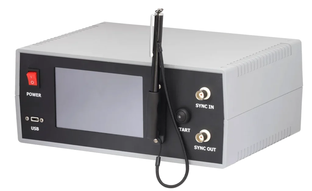
The SDC-BT pulsed laser diode driver series is expertly engineered to power medium-power diode-pumped solid-state (DPSS) lasers, including Nd:YAG systems. Delivering highly reliable performance, this module supplies a pulsed current with precision pulse widths ranging from 50 to 300 µs to effectively drive pump diodes, generating up to 100 W of average power. The system fully supports pulse repetition rates of up to 50 Hz for high-voltage models and 100 Hz for low-voltage models.
For maximum operational flexibility, the SDC-BT offers two distinct synchronization modes:
-
Internal: Pulse generation is precisely governed by the system’s internal clock.
-
External: Pulses featuring a user-defined width are triggered via an external synchronization signal.
Additionally, this robust unit is fully capable of powering and controlling a Pockels cell driver for the generation of Q-switched pulses. Designed for seamless system integration, the SDC-BT can transmit output synchronization signals to ancillary equipment. Custom configurations, including multiple outputs, are readily available upon request to meet specific technical requirements.
Power management is simplified with a universal 110-240 V AC wide-range input. Operators can easily configure all critical parameters for the SDC-BT laser diode driver—including output current, buffer voltage, pulse width, and pulse repetition rate—directly through the intuitive 5” color touchscreen display on the front panel. Alternatively, the driver supports comprehensive computer control via USB or the default RS-485 interface (RS-232 connectivity is also available upon request).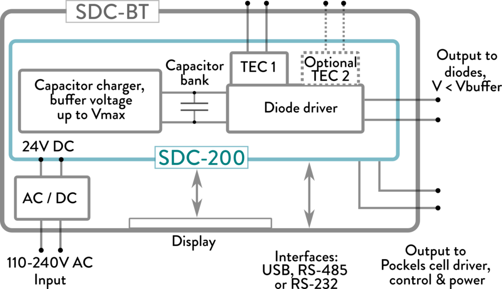
Technical Specifications
| INPUT | |
|---|---|
| Voltage | 110-240 VAC, 50/60 Hz, 1 ph |
| Current consumption | < 5 A @ 110 V AC |
| OUTPUT | |
| Regime of operation | pulsed |
| Maximum buffer voltage (Vmax) | model dependent (user selectable up to 450 V), other on request |
| Maximum output voltage | model dependent (see also How to order?), other on request |
| Maximum output current (Imax or I250) | model dependent (user selectable up to 400 A), other on request Imax is fully achievable at pulse widths up to 250 us, and is derated at longer pulses |
| Output current | approx. 10-100 % of Imax adjustable, other on request |
| Buffer voltage | adjustable in 10 V – Vmax range, other on request |
| Pulse width | adjustable in 50 us – Tmax range, Tmax is 300 us by default, other on request |
| Rise time | < 20-30 us typically, slow start ramp adjustable in 0-50 us range |
| Pulse repetition rate | up to 50/100 Hz adjustable, other on request |
| Maximum average output power | 100 W, model dependent, other on request |
| Peak power | model dependent (usually in the 20-50 kW range), other on request |
| Bias current | +, model dependent (~50-100 mA) |
| TEC 1 | |
| Current | up to 10 A |
| Voltage | up to 20 V |
| Power | 200 W max. |
| Feedback loop | 10 kOhm NTC |
| Temperature | +10 … +40 °C by default, other on request |
| TEC 2 | |
| Current | up to 5 A |
| Voltage | up to 20 V |
| Power | 50 W max. |
| Feedback loop | 10 kOhm NTC |
| Temperature | +10 … +40 °C by default, other on request |
| MISCELLANEOUS | |
| Protections | • from overheating • from incorrect buffer voltage • TEC1 out of range • TEC2 out of range • too high input frequency • door-interlock connection |
| Cooling | forced-air cooling with built-in fans |
| Interfaces | • UI – 5” display with touchscreen • USB • RS-485 (RS-232 on request) interface |
| Synchronizations | • 1 pc synchro input • 1 pc synchro output |
| Pockels cell driver control | yes, the Pockels cell driver needs to be purchased separately, placed outside and connected with a cable |
| ENVIRONMENT | |
| Operating temperature | +10 … +40 °C |
| Storage temperature | -20 … +60 °C |
| Humidity | 0 … 90%, non-condensing |
| OTHER | |
| Size (LxWxH) | 260x195x107 mm |
| Weight | < 3.0 kg |
Options
Different customizations (e.g. non-standard output currents, non-standard diode voltages, software customizations, Pockels cell driver control) are possible on request.
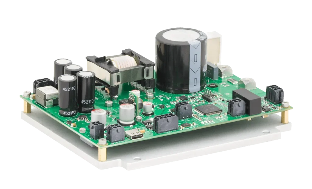
Embedded version of the SDC-BT is available under the name SDC-200 .
SDC-200:
How To Order
SDC-BT-XXXX-[YYYY]-[VVVVV], where:
- XXXX code denotes the voltage version of the driver (nominal value, can be 63 V, 80 V, 100 V, 126 V, 160 V, 200 V, 250 V, 400 V, 450 V, or custom). The maximum output current, internal capacitor bank capacitance, average output power, and number of TECs are fixed for each voltage version, see details in the table below.
- YYYY defines low‑current and high‑current versions of the driver. The low‑current versions are optimized for low‑current diodes and for operating regimes with low energy but high repetition rates. It is reasonable to choose a low‑current version, which provides improved output‑current quality in the low‑current region, if the maximum operating current in your system is at least three times lower than the Imax of the standard model. If not specified, the standard version is supplied.
- VVVVV code denotes the type of communication interface, it can be either RS232 or RS485. By default, the RS485 version is supplied.
| PARAMETER | VALUE (1) | |||
|---|---|---|---|---|
| SDC-BT-63V | SDC-BT-80V | SDC-BT-100V | SDC-BT-126V | |
| Embedded capacitor bank: | ||||
| Voltage (Vmax), V | 63 | 80 | 100 | 126 |
| Capacitance, mF | 10.8 | 10.8 | 6.0 | 3.6 |
| Capacitor charging power supply: |
||||
| Buffer voltage, V | 10…63 | 10…80 | 10…100 | 10…126 |
| Maximum power in dependence on buffer voltage, W (2) |
> 100 @ 30V…63V |
> 100 @ 30V…80V |
> 100 @ 30V…100V |
> 100 @ 30V…126V |
| Diode driver: | ||||
| Maximum output current, A: – @ 250 us (I250) – @ 300 us (I300) |
350 300 |
350 300 |
300 250 |
250 200 |
| Minimum output current, A | 10 | |||
| Recommended diode voltage, V (3): – @ I300, 300 us – @ ½I250, 250 us |
< 47 < 50 |
< 63 < 69 |
< 79 < 87 |
< 96 < 107 |
| Maximum pulse width (Tmax), us | 300 | |||
| Minimum pulse width, us | 50 | |||
| Maximum repetition rate, Hz (4) | 100 | |||
| Output limitations: | ||||
| Pulse energy limit, J I300*Vmax*Tmax |
~5.6 | ~7.2 | ~7.5 | ~7.5 |
| Power limit, W | 100 | |||
| Guaranteed regime | 300A-46V- 300us-15Hz or 100A-25V- 250us-100Hz |
300A-63V- 300us-10Hz or 100A-25V- 250us-100Hz |
250A-79V- 300us-10Hz or 100A-25V- 250us-100Hz |
200A-96V- 300us-10Hz or 100A-25V- 250us-100Hz |
| TEC 1 | + | + | + | + |
| TEC 2 | + | + | + | + |
| Low-current versions | SDC-BT-63V-100A | SDC-BT-80V-100A | on request | on request |
| I250 / I300, A | 100 / 100 | 100 / 100 | – | – |
| Imin, A | 5 | 5 | – | – |
| High-current versions | SDC-BT-63V-400A | SDC-BT-80V-400A | on request | on request |
| Capacitance, mF | 14.4 | 14.4 | – | – |
| I250 / I300, A | 400 / 350 | 400 / 350 | – | – |
| Imin, A | 10 | 10 | – | – |
| Recommended diode voltage, V (3): – @ I300, 300 us – @ ½I250, 250 us |
< 46 < 52 |
< 63 < 69 |
– | – |
| Guaranteed regime | 400A-44V- 250us-10Hz or 350A-44V- 300us-10Hz |
400A-44V- 250us-10Hz or 350A-44V- 300us-10Hz |
– | – |
(1) Customizations (e.g. non-standard output currents, non-standard diode voltages and other parameters, software customizations, Pockels cell driver control customizations) are possible on request.
(2) In dependence on the topology of the internal DC/DC power converter the dependence of the output power of the capacitor charger from the output voltage is principally different for different models of SDC-BT. Two low-voltage models deliver full output power in a wide range of the output voltages. Unlike them, two high-voltage models are able to deliver full output power close to Vmax only. At lower output voltages the output power of high-voltage models drops approx. linearly with decreasing output voltage.
(3) Please note that the output voltage applied to the diodes is several volts lower than the buffer voltage due to voltage drops across internal components and wiring. The higher output current and pulse width are, the lower output voltage is possible with the same buffer voltage. On the contrary, the possible output voltage reaches exactly the buffer voltage at very low currents and pulse widths.
(4) If the diode voltage is close to Vmax and the operating current is close to Imax, the typical pulse energy is ~5–7 J, and 100 Hz operation is not possible due to the 100 W average power limitation. Therefore, 100 Hz operation is only possible when the operating current and/or voltage are several times lower than Imax and Vmax, respectively. In such cases, it may be reasonable to consider a low‑current version of the driver.
Examples:
– SDC-BT-63V – fully standard 63 V version with all the parameters as given above
– SDC-BT-63V-100A-RS232 – low-current version of 63 V model with RS-232 communication interface instead of RS-485
| PARAMETER | VALUE (1) | |||
|---|---|---|---|---|
| SDC-BT-160V | SDC-BT-200V | SDC-BT-250V | SDC-BT-400V | |
| Embedded capacitor bank: | ||||
| Voltage (Vmax), V | 160 | 200 | 250 | 400 |
| Capacitance, uF | 2700 | 2200 | 1500 | 820 |
| Capacitor charging power supply: |
||||
| Buffer voltage, V | 10…160 | 10…200 | 10…250 | 10…400 |
| Maximum power in dependence on buffer voltage, W (2) |
> 100 @ 160V |
> 100 @ 200V |
> 100 @ 250V |
> 100 @ 400V |
| Diode driver: | ||||
| Maximum output current, A: – @ 250 us (I250) – @ 300 us (I300) |
225 200 |
200 175 |
175 150 |
125 100 |
| Minimum output current, A | 10 | 10 | 10 | 5 |
| Recommended diode voltage, V (3): – @ I300, 300 us – @ ½I250, 250 us |
< 118 < 137 |
< 144 < 161 |
< 196 < 223 |
< 333 < 357 |
| Maximum pulse width (Tmax), us | 300 | |||
| Minimum pulse width, us | 50 | |||
| Maximum repetition rate, Hz (4) | 50 | |||
| Output limitations: | ||||
| Pulse energy limit, J I300*Vmax*Tmax |
~9.6 | ~10.5 | ~11.2 | ~12.0 |
| Power limit, W | 100 | |||
| Guaranteed regime | 225A-137V- 250us-10Hz or 110A-140V- 250us-20Hz or 50A-120V- 250us-50Hz |
200A-160V- 250us-10Hz or 100A-150V- 250us-20Hz or 50A-110V- 250us-50Hz |
150A-195V- 250us-10Hz or 100A-148V- 250us-20Hz or 50A-105V- 250us-50Hz |
100A-330V- 250us-10Hz or 50A-360V- 250us-20Hz or 50A-100V- 250us-50Hz |
| TEC 1 | + | + | + | + |
| TEC 2 | N/A | |||
| Alternative versions | on request | on request | on request | SDC-BT-450V |
| Capacitance, uF | – | – | – | 780 |
| I250 / I300, A | – | – | – | 125 / 100 |
| Imin, A | – | – | – | 5 |
| Recommended diode voltage, V (3): – @ I300, 300 us – @ ½I250, 250 us |
– | – | – | < 371 < 403 |
| Guaranteed regime | – | – | – | 100A-330V- 250us-10Hz or 50A-360V- 250us-20Hz or 50A-120V- 250us-50Hz |
(1) Customizations (e.g. non-standard output currents, non-standard diode voltages and other parameters, software customizations, Pockels cell driver control customizations) are possible on request.
(2) In dependence on the topology of the internal DC/DC power converter the dependence of the output power of the capacitor charger from the output voltage is principally different for different models of SDC-BT. Two low-voltage models deliver full output power in a wide range of the output voltages. Unlike them, two high-voltage models are able to deliver full output power close to Vmax only. At lower output voltages the output power of high-voltage models drops approx. linearly with decreasing output voltage.
(3) Please note that the output voltage applied to the diodes is several volts lower than the buffer voltage due to voltage drops across internal components and wiring. The higher output current and pulse width are, the lower output voltage is possible with the same buffer voltage. On the contrary, the possible output voltage reaches exactly the buffer voltage at very low currents and pulse widths.
(4) If the diode voltage is close to Vmax and the operating current is close to Imax, the typical pulse energy is ~10–15 J, and 50 Hz operation is not possible due to the 100 W average power limitation. Therefore, 50 Hz operation is only possible when the operating current and/or voltage are several times lower than Imax and Vmax, respectively. In such cases, it may be reasonable to consider a low‑current version of the driver.
Examples:
– SDC-BT-400V – fully standard 400 V version with all the parameters as given above
– SDC-BT-250V-RS232 – standard 250V version, but with RS-232 communication interface