- High-Voltage Amplitude 1………………………………………………………………………………… 2800 ÷ 3800 V
- HV Pulse-to-Pulse Instability…………………………………………………………………………….. 5 %
- Max Current During Pulse…………………………………………………………………………………. 40 A
- Max Capacitance……………………………………………………………………………………………….. 40pF
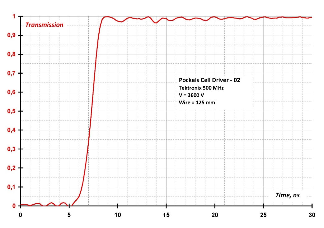
- Rising Front Duration 2 ……………………………………………………………………………………. 1 ÷ 2 nsec
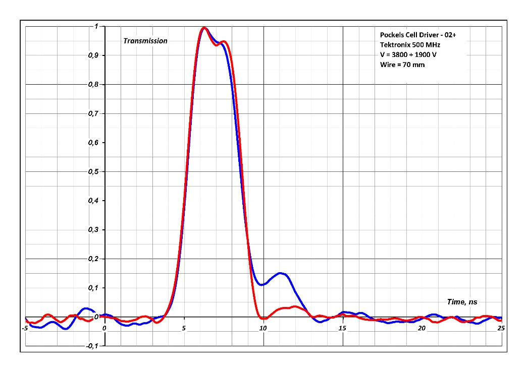
- HV Pulsewidth (factory-set) 3 ………………………………………………………………………….. 0.5 ÷ 2 μsec
- Falling Front Duration……………………………………………………………………………………… 1 ÷ 2 μsec
- Max Repetition Rate (Frequency)
- With 4.6 mm transformer………………………………………………………………………… 2 kHz
- With 9.2 mm transformer………………………………………………………………………… 5 kHz
- Input TTL Signal Amplitude…………………………………………………………………………….. 3 ÷ 12 V
- HV Pulse delay Vs. TTL trigger pulse 4…………………………………………………………….. 15 ÷ 30 nsec
- Timing Jitter of the HV Pulse Vs. Trigger…………………………………………………………. < 900 psec
- DC Voltage to power the driver………………………………………………………………………… 4.5 ÷ 7.5 V
- Current
- 2kHz …………………………………………………………………………………………………………. 250 mA
- 5kHz ………………………………………………………………………………………………………… 400 mA
- Working Temperature Range……………………………………………………………………………. –40 ÷ +60°C
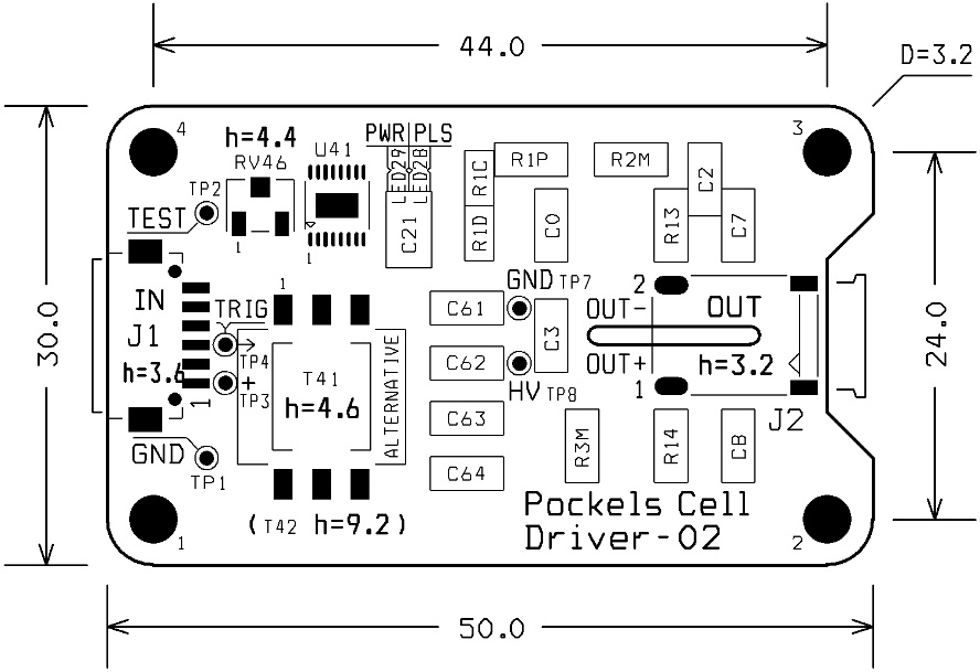
- Dimensions …………………………………………………………………………………………………….. 30 × 50 × 8 mm3
- Mounting Hole Pattern (Ø 3.2 mm) ………………………………………………………………… 24 × 44 mm
1 Is set from the built-in potentiometer or remotely.
2 Depends on the load inductance and HV amplitude.
3 Set during fabrication.
4 Delay depends on the TTL pulse. The higher trigger amplitude, the shorter delay.
Pockels Cell Driver PCDA4-02 Connection Diagram
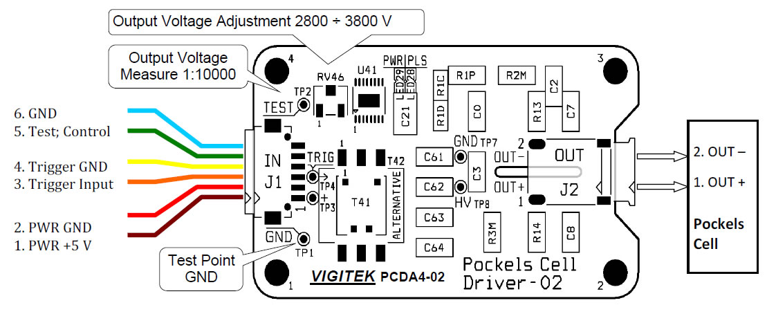
Connector J1 (input):
Pin 1 (brown) – power supply + 5 V & 250 mA;
Pin 2 (red) – power supply GND;
Pin 3 (orange) – trigger input + (3 ÷ 8) V & 25 mA; rising edge < 50 ns; duration > 50 ns;
Pin 4 (yellow) – trigger GND;
Pin 5 (green) – output voltage measure signal; DC voltage scale 1:10000;
Pin 6 (blue) – output voltage measure GND.
Connector J2 (output):
Pin 1 (HV blue) – negative high voltage output;
Pin 2 (HV red) – positive high voltage output.
Note 1.
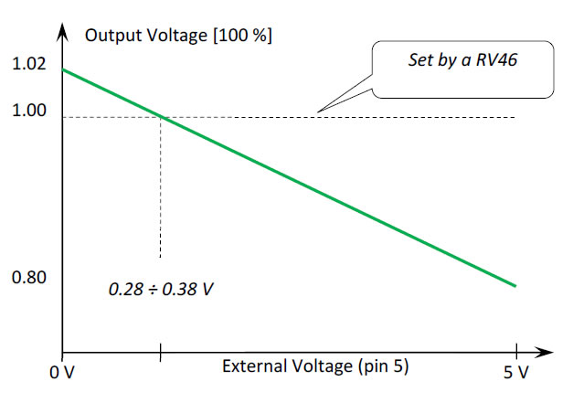
Pins 5 and 6 can be used for the remote adjustment of the HV pulse’ amplitude relative to the value set by potentiometer RV46 within a range of +2% to -20%.
That is, if a voltage of U=0V is applied from the external source to pin 5. – then HV amplitude would be ~2% higher than nominal setting.
If U=5V is applied to pin 5, then amplitude would be lower by ~20%. The input impe- dance of the pin 5 is ~26kΩ.
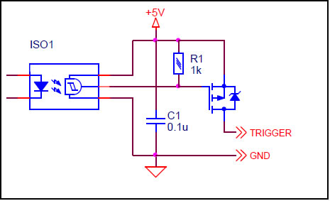
To correctly operate driver PCDA4-02, it must be triggered by the electric pulse with following
parameters:
- The amplitude of the trigger-pulse (on pin 3 of connector J1) must be higher than 3V, and
preferably 5V (permitted up to 12V). - Rise time of the trigger-pulse (on pin 3 of connector J1) must be shorter than 50 nsec.
- Need to provide the input current (on pin 3 of connector J1) higher than 25 mA. This will require a powerful and fast signal generator.
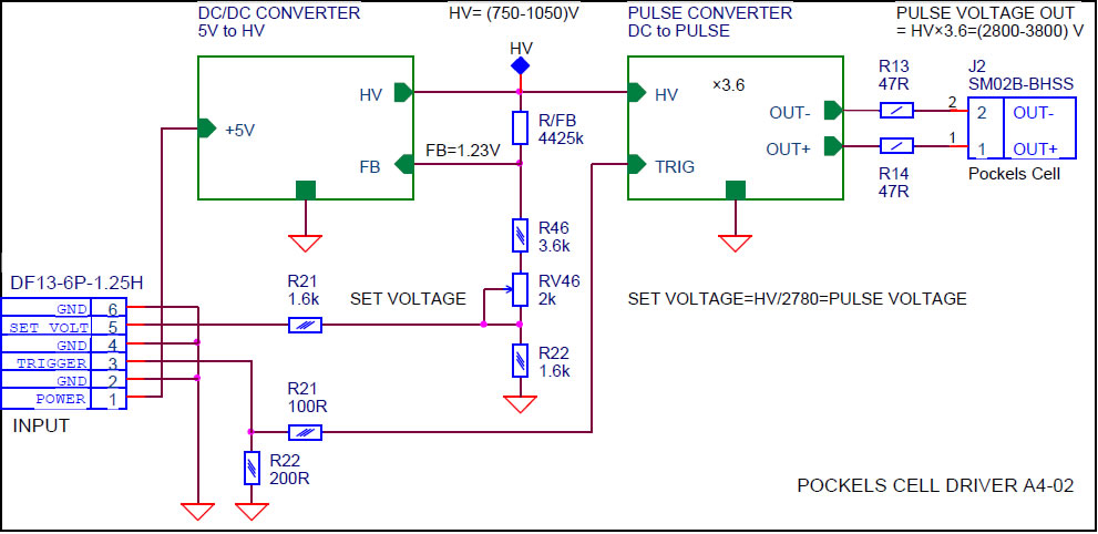
Electric Block-Diagram of «Pockels Cell Driver – PCDA4-02»
- If an isolated trigger pulse is required, it’s necessary to use opto-couple with logic output, for example HCPL-2611 or OPI1268. Digital isolators type Si8710 or Si8610 can also be used.
Output waveform of the Pockels Cell Driver – 02
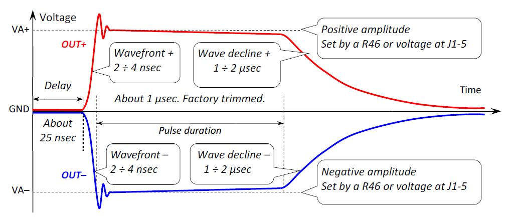
Low-voltage indirect (non-touching) monitoring of the output pulse waveform:
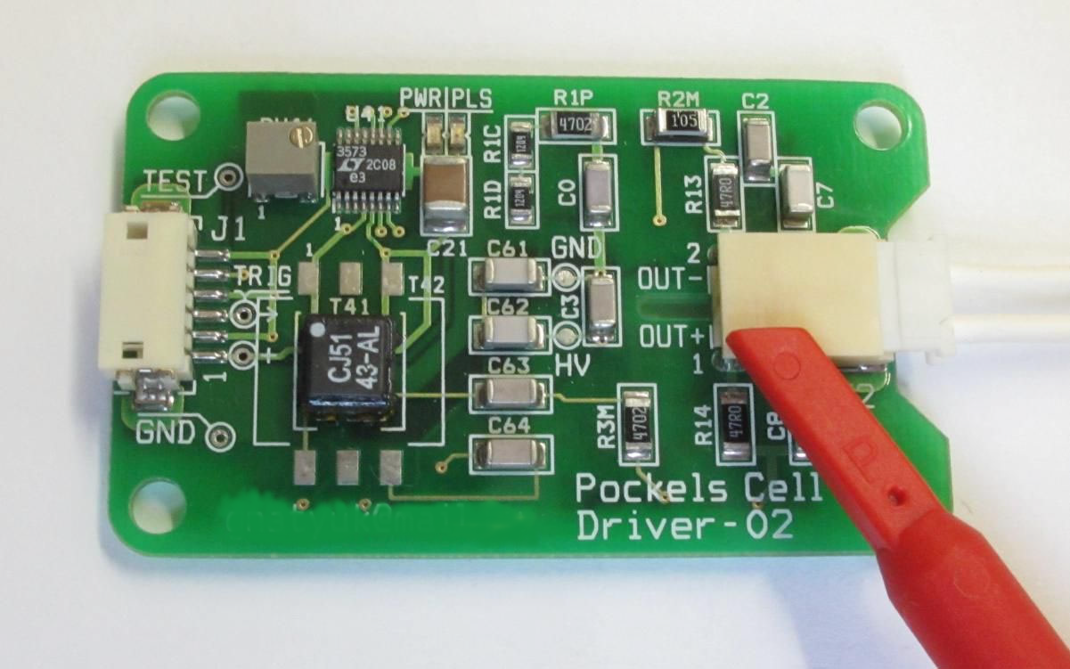
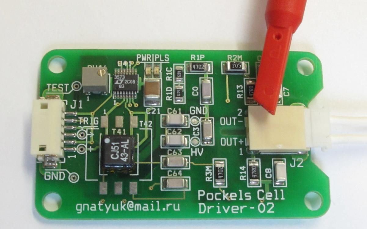
Oscilloscope probe (1:10) must be placed in close proximity to the pin 1 of the HV connector J2 (or resistors R14), in the next place to the pin 2 of the HV connector J2 (or resistors R13), but without actually touching it. The scale of the oscilloscope must be set on the 1 ÷ 10 V/D.
High-voltage low-frequency measurement of the output voltage:
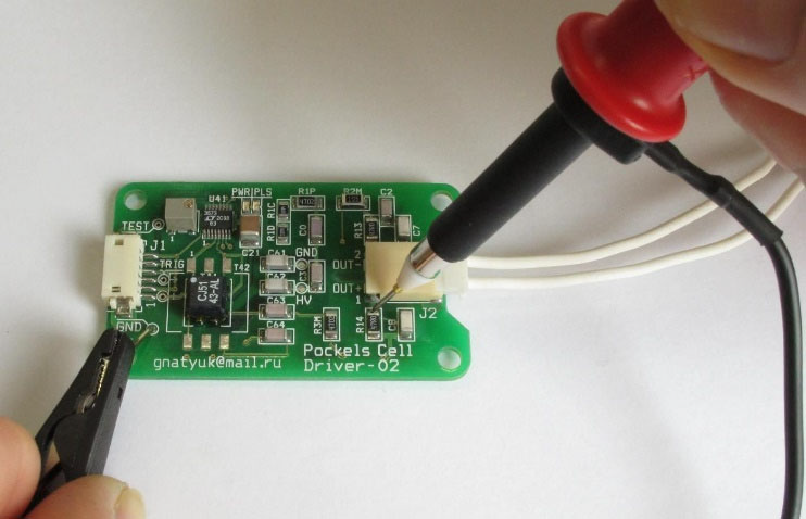
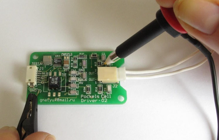
Measurements can be made simultaneously by the two probes.
Output voltage – the sum of two measurements.
High-voltage high-frequency measurement of the output voltage:
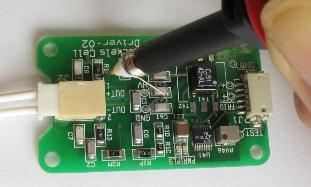
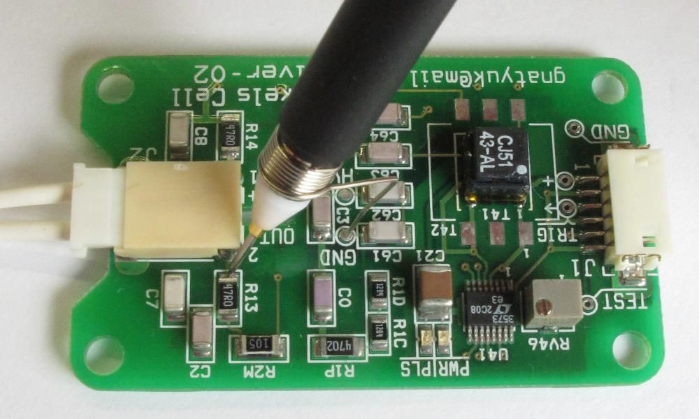
Measurements can be made simultaneously by the two probes.
Output voltage – the sum of two measurements.
