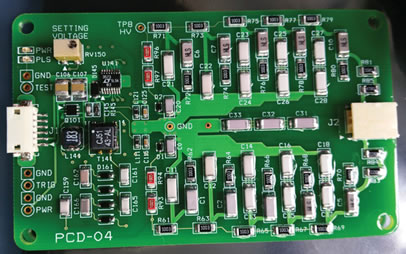
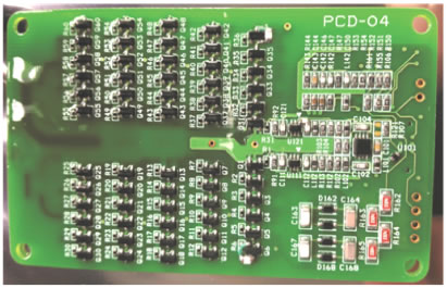
-
- Output voltage amplitude1 ……………………………………………………………….. 3200 ÷ 5800 V
- Output voltage pulse-to-pulse instability …………………………………… 1 %
- Max pulse current ………………………………………………………………………………… 40 A
- Max load capacitance …………………………………………………………………………. 30 pF
- HV pulse rise time2 ……………………………………………………………………………… 1 ÷ 2 nsec
- HV pulse fall time2 ……………………………………………………………………………….. 1 ÷ 2 nsec
- HV pulse duration3 ……………………………………………………………………………… 40 ÷ 1000 nsec
- Max HV pulse repetition rate ………………………………………………………….. 1 kHz
- Trigger voltage (input impedance is 50 Ohms) ……………………….. 4.5 ÷ 5.5 V (+5V)
- Output pulse delay vs. trigger pulse 4 …………………………………………. 10 ÷ 20 nsec
- HV pulse jitter ……………………………………………………………………………………….. < 0.5 nsec
- External powering requirements:
- DC supply voltage…………………………………………………………………………………. 4.75 ÷ 5.25 V (+5V)
- DC supply current ……………………………………………………………………………….. 400 mA max
- Operating temperature range …………………………………………………………. –40 ÷ +60 °C
- Dimensions (see dimensional drawing below)…………………………. 80 × 50 × 12 mm3
- Mounting hole pattern (Æ3.2 mm) ……………………………………………….. 74 × 44 mm
1 Is set from the built-in potentiometer.
2 Depends on the load impedance and output voltage amplitude.
3 Determined by an external trigger-generator.
4 Delay depends on the trigger pulse. The shorter trigger rise and higher trigger amplitude the shorter delay.
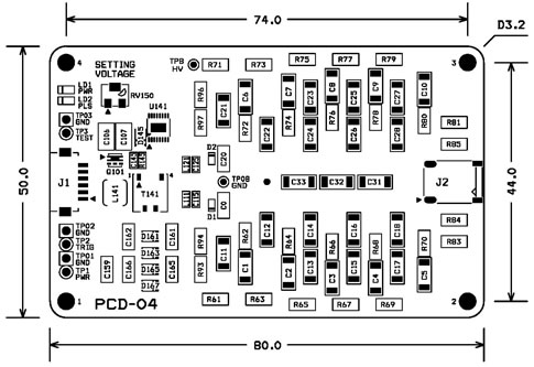
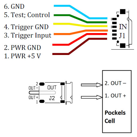
Connector J1 (input) – DF13-6P-1.25H (Hirose):
Pin 1 – power supply + 5V & 400 mA max;
Pin 2 – power supply GND;
Pin 3 – trigger input +5V; input impedance 50Ω; duration >40 nsec;
Pin 4 – trigger GND;
Pin 5 – measurement of the output voltage amplitudes; DC voltage scale 1:10000;
Pin 6 – output voltage measure GND.
Connector J2 (output) – SM02B-BHSS (JST):
Pin 1 – first high voltage output;
Pin 2 – second high voltage output.
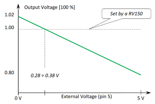
Pins 5 and 6 can be used for the remote adjustment of the HV pulse’ amplitude relative to the value set by potentiometer RV46 within a range of +2% to -20%.
That is, if a voltage of U=0V is applied from the external source to pin 5, – then HV amplitude would be ~2% higher than nominal setting.If U=5V is applied to pin 5, then amplitude would be lower by ~20%. The input impedance of the pin 5 is ~45kΩ.
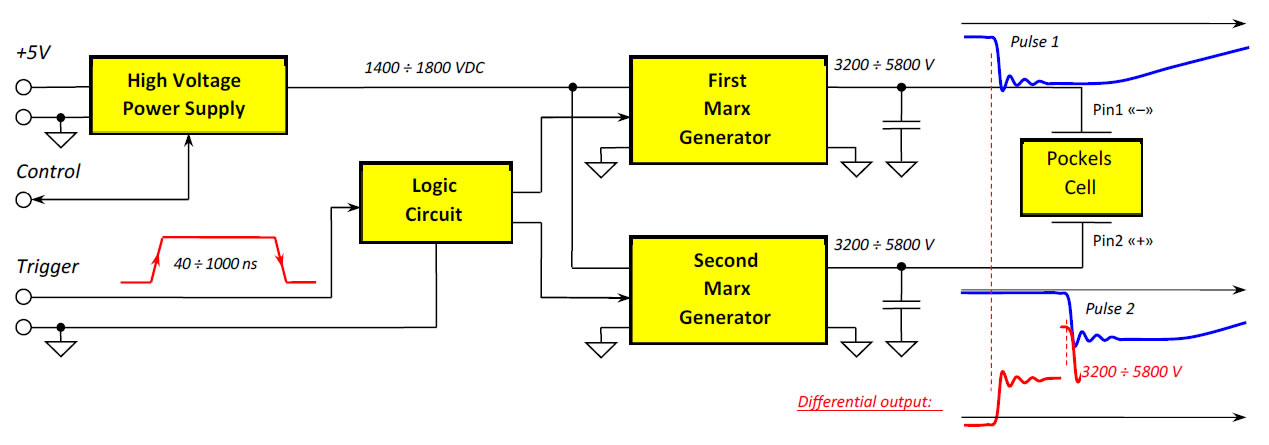
BLOCK DIAGRAM OF PCD-04 – PULSE DURATION IS DETERMINED BY THE TRIGGER PULSE
TIMING DIAGRAM OF MODIFIED PCD-04 FOR TWO-STEPS, HALF-WAVE VOLTAGE APPLICATIONS IN THE REGENERATIVE AMPLIFIERS (RA)
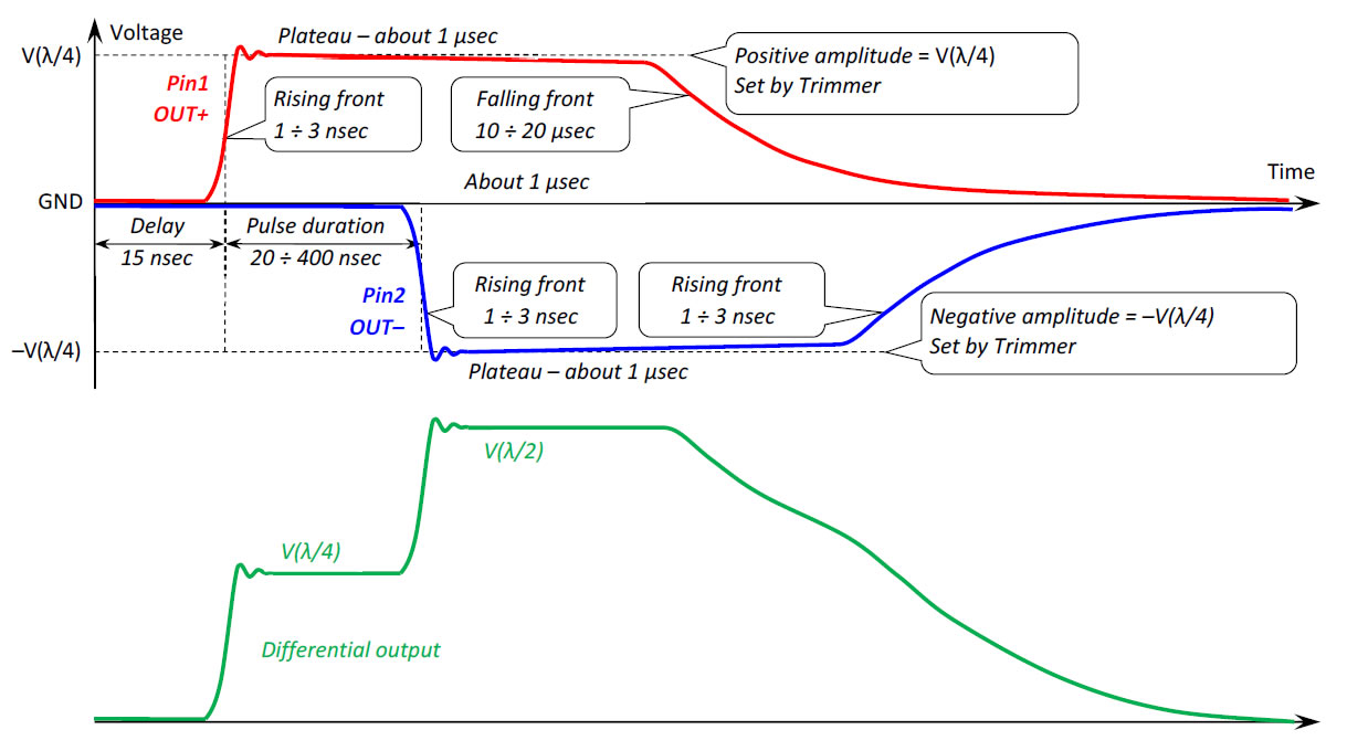
PULSE I [V(λ/4)] – INJECTION SEEDING OF THE RA
PULSE II [V(λ/2)] – EJECTION (“DUMPING”) OF THE AMPLIFIED LASER PULSE OUT OF RA
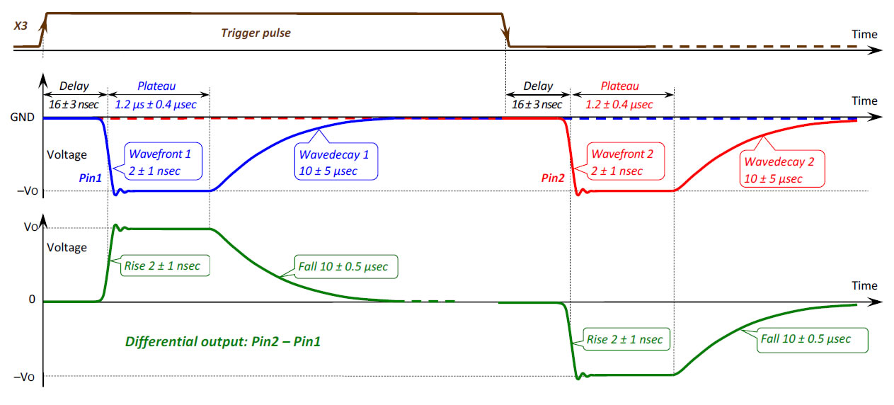
As an option, the driver PCD-04 can produce HV pulses of a different polarity, if duration of the trigger-pulse exceeds 50 μsec. If rectangular trigger pulses of 500 μsec duration are applied with 1 msec period, then driver will produce HV pulses of the opposite polarity with frequency 1kHz (see Fig. on page 4). This will require 12 VDC supply and a conventional pulse generator.
OUTPUT WAVEFORM OF PCD-04 (TRIGGER PULSE DURATION > 100 μsec)
