- Output amplitude of the first step 1 ………………………………………………………………………. 2800 ÷ 3600 V
- Output amplitude of the second step (double voltage of first step) 1 ……………………. 5600 ÷ 7200 V
- Unevenness of the amplitude on the plateau ……………………………………………………….. < 5 %
- Output voltage pulse-to-pulse instability ……………………………………………………………… < 1 %
- Max pulsed current …………………………………………………………………………………………………. 20 A
- Optimal load capacitance ………………………………………………………………………………………. 4 ÷ 12 pF
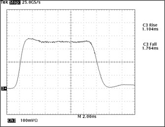
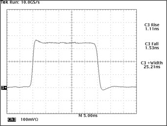
- HV pulse rise time of first step 2 ……………………………………………………………………………. 1 ÷ 3 nsec
- HV pulse rise time of second step 2 ………………………………………………………………………. 1 ÷ 3 nsec
- Pulse duration of the first step 3 ……………………………………………………………………………. 2 ÷ 600 nsec
- Duration of the second step plateau …………………………………………………………………….. ≈ 1000 nsec
- Max HV pulse repetition rate 2 ……………………………………………………………………………… 1000 Hz
- Trigger voltage (input impedance is 50 Ω) ……………………………………………………………. 5V (4.5 ÷ 5.5 V)
- Output pulse delay vs. trigger pulse 4 …………………………………………………………………… 15 ÷ 20 nsec
- HV pulse jitter ………………………………………………………………………………………………………. < 0.2 nsec
- External power supply voltage ………………………………………………………………………………. 12 VDC (8 ÷ 16 VDC)
- External power supply current ……………………………………………………………………………….. 500 mA
- Operating temperature range ……………………………………………………………………………….. –40 ÷ +60 °C
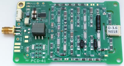
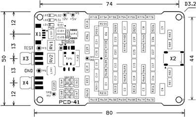
- Dimensions ……………………………………………………………………………………………………………… 80 × 50 × 15 mm
- Mounting hole pattern (Ø 3.2 mm) ……………………………………………………………………….. 74 × 44 mm
- Weight (OEM version) ……………………………………………………………………………………………. 100 g
1 HV amplitude is controlled by built-in trimmer RV1. The range of voltage corresponds to a specific driver model.
2 Depends on the load impedance and output voltage amplitude.
3 Is determined by an external trigger-generator.
4 Delay depends on the trigger pulse and HV output amplitudes. The higher the HV output amplitude, the shorter delay.
Connection diagram
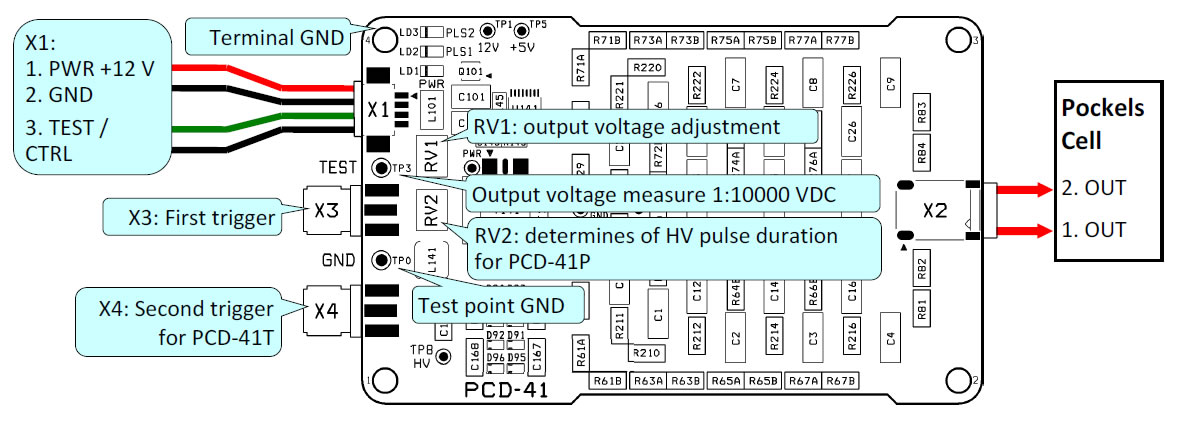
Connector X1 (input) – 53261-0471 (Molex) :
Pin 1 (red) – power supply + 12 V & 500 mA max;
Pin 2 (black) – power supply GND;
Pin 3 (green) – output voltage measure signal; DC voltage scale 1:10000; NOTE 1
Pin 4 (black) – output voltage measure GND.
Connector X2 (output) – SM02B-BHSS (JST) :
Pin 1 (HV red) – first high voltage output;
Pin 2 (HV red) – second high voltage output.
Connector X3, X4 (input) – SMA-J-P-H-ST-EM1 (Samtec) :
Trigger pulse input +5 V; impedance 50 Ω.
Connector X3 – input trigger pulse determines output HV pulse duration for first step.
Connector X4 – not available.
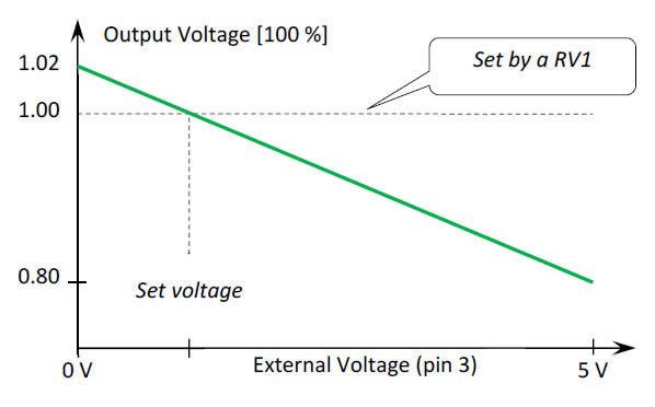
Note 1. Pin 3 and Pin 4 can be used for setting the amplitude of output voltage pulse from –20 % to +2 % (relative to value have been set by trimmer RV1).
If 0 V is set on Pin 3 from an external source, the pulse amplitude will be ~2 % higher than the set value.
If 5 V is set on the Pin 3, the pulse amplitude will be lower by ~20 %.
The input impedance of the Pin 3 is 45kΩ.
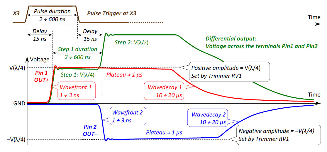
OUTPUT WAVEFORM OF PCD-041D – TWO-STEP PULSE WITH VOLTAGE DOUBLING
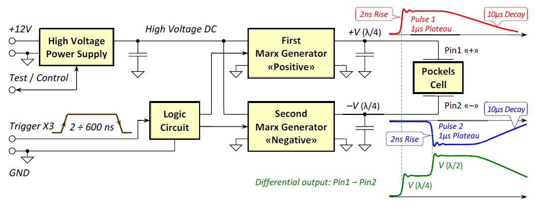
Block diagram of PCD-041D – two-step pulse with voltage doubling
Waveforms of the transmitted light beam
Pulse voltage: V0UT = 2 × 3600 V; Pockels cell half-wave voltage: Vλ/2 = 3800 V
