Technical Specifications
Output high voltage amplitude 1
-
-
- PCD-041-4800 (can be extended to 5800 V)
- 3600 ÷ 4800 V
-
- PCD-041-3800
- 2600 ÷ 3800 V
-
- PCD-041-2800
- 1800 ÷ 2800 V
-
- PCD-041-2000
- 1300 ÷ 2000 V
-
-
- Inhomogeneity of the amplitude on the plateau
- < 5 %
-
- Output voltage pulse-to-pulse instability
- < 1 %
-
- Max pulsed current
- 20 A
-
- Optimal load capacitance
- 4 ÷ 10 pF
-
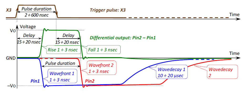
- HV pulse rise time 2
- 1 ÷ 3 nsec
-
- HV pulse fall time 2
- 1 ÷ 3 nsec
-
- HV pulse duration 3
- 2 ÷ 600 nsec
-
- Max HV pulse repetition rate 2
- 2000 Hz
-
- Trigger voltage (input impedance is 50 Ω)
- 5V (4.5 ÷ 5.5 V)
-
- Output pulse delay vs. trigger pulse 4
- 15 ÷ 20 nsec
-
- HV pulse jitter
- < 0.2 nsec
-
- External power supply voltage
- 12 VDC (8 ÷ 16 VDC)
-
- External power supply current
- 500 mA
-
- Operating temperature range
- –40 ÷ +60 °C
-
- Dimensions
- 80 × 50 × 15 mm
-
- Mounting hole pattern (Ø3.2 mm)
- 74 × 44 mm
-
- Weight (OEM version)
- 100 g
1 HV amplitude is controlled by built-in trimmer RV1. The range of voltage corresponds to a specific driver model.
2 Depends on the load impedance and output voltage amplitude.
3 Determined by an external trigger-generator. For version PCD-041P pulsewidth is 2 ÷ 10 nsec (controlled by trimmer RV2).
4 Delay depends on the trigger pulse and HV output amplitudes. The higher the HV output amplitude, the shorter delay.
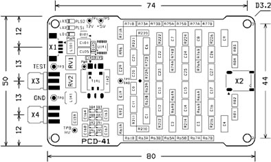
CONNECTION DIAGRAM
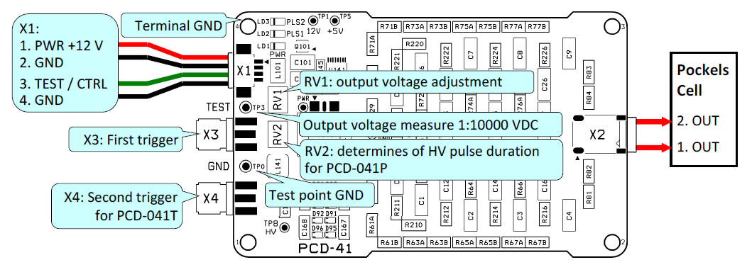
Connector X1 (input) – 53261-0471 (Molex) :
Pin 1 (red) – power supply + 12 V & 500 mA max;
Pin 2 (black) – power supply GND;
Pin 3 (green) – output voltage measure signal; DC voltage scale 1:10000; NOTE 1
Pin 4 (black) – output voltage measure GND.
Connector X2 (output) – SM02B-BHSS (JST) :
Pin 1 (HV red) – first high voltage output;
Pin 2 (HV red) – second high voltage output.
Connector X3, X4 (input) – SMA-J-P-H-ST-EM1 (Samtec) :
Trigger pulse input +5 V; impedance 50 Ω.
For PCD-041 – HV pulse duration is determined by duration of trigger pulse on X3.
Connector X3 – input trigger pulse determines output HV pulse duration.
Connector X4 – not available.
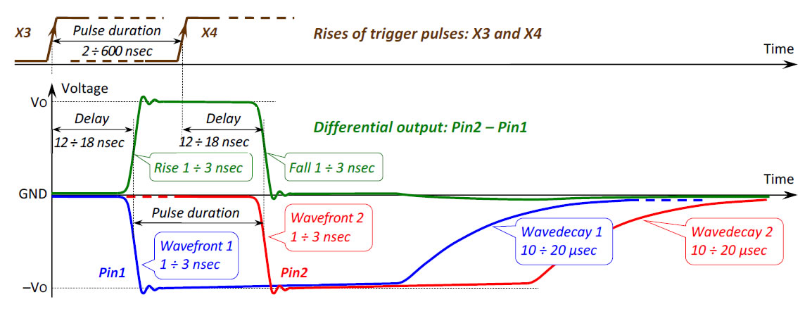
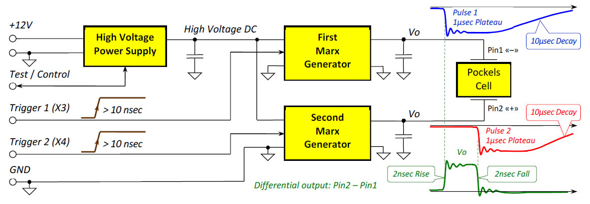
For PCD-041T – HV pulse duration is determined by delay between rises of trigger pulses on X3 and X4.
Connector X3 – rising edge of input trigger pulse initiates front of output HV pulse.
Connector X4 – rising edge of input trigger pulse initiates falling edge of output HV pulse.
Trigger pulses at X3 and X4 are fully interchangeable. First in time pulse initiates rising edge of HV out-put pulse while second one initiates falling edge of HV pulse.
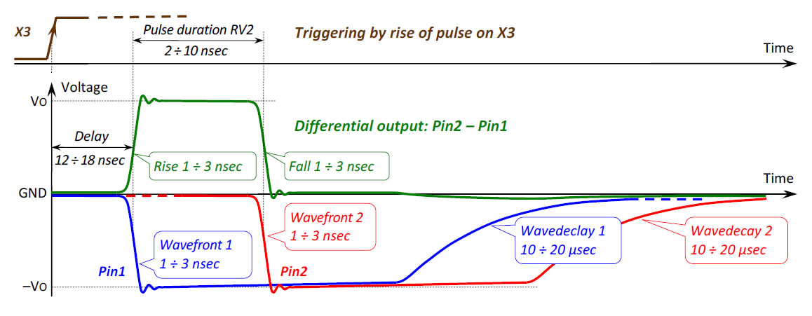
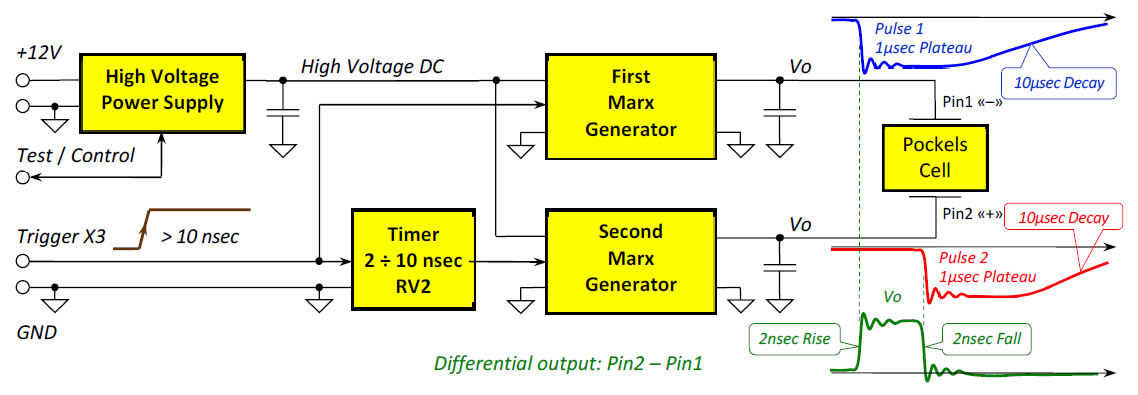
For PCD-041P – Pulse picker. HV pulse duration is 2 ÷ 10 ns and controlled by trimmer RV2.
Connector X3 – rising edge of input trigger pulse initiates front of output HV pulse.
Connector X4 – not available.
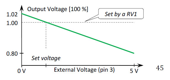
Note 1. Pin 3 and Pin 4 can be used for setting the amplitude of output voltage pulse from –20 % to +2 % (relative to value have been set by trimmer RV1).
If 0 V is set on Pin 3 from an external source, the pulse amplitude will be ~2 % higher than the set value.
If 5 V is set on the Pin 3, the pulse amplitude will be lower by ~20 %. The input impedance of the Pin 3 is 45 kΩ.
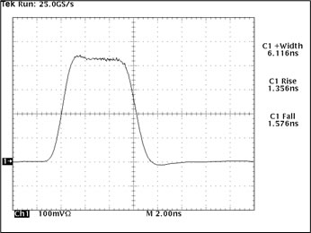
OUTPUT WAVEFORM OF PCD-041 – PULSE DURATION IS DETERMINED BY ONE TRIGGER PULSE AT X3
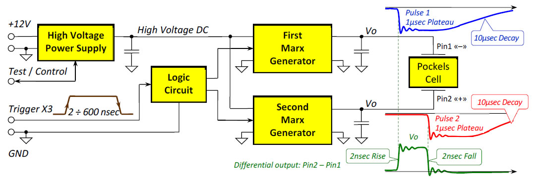
Block diagram of PCD-41 – pulse duration is determined by one trigger pulse at X3
WAVEFORMS OF THE TRANSMITTED LIGHT BEAM
Pulse voltage: V0 = 3800 V; Pockels cell half-wave voltage: Vλ/2 = 3800 V
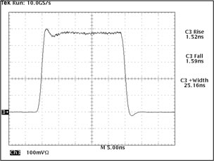
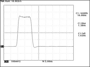
Output waveform of PCD-041T – pulse duration is determined by two trigger pulses at X3 & X4
BLOCK DIAGRAM OF PCD-041T – PULSE DURATION IS DETERMINED BY TWO TRIGGER PULSES AT X3 & X4
Waveforms of the transmitted light beam
Pulse voltage: V0 = 3800 V; Pockels cell half-wave voltage: Vλ/2 = 3800 V
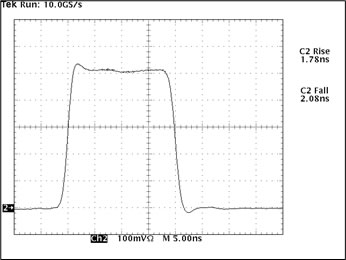
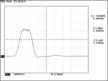
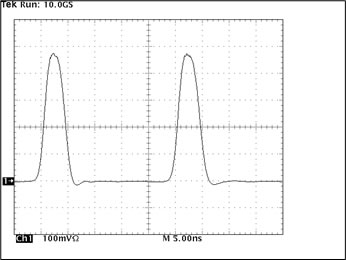
Output waveform of PCD-041P – pulse duration is controlled by trimmer RV2
BLOCK DIAGRAM OF PCD-041P – PULSE DURATION IS CONTROLLED BY TRIMMER RV2
WAVEFORMS OF THE TRANSMITTED LIGHT BEAM
Pulse voltage: V0 = 3800 V; Pockels cell half-wave voltage: Vλ/2 = 3800 V
